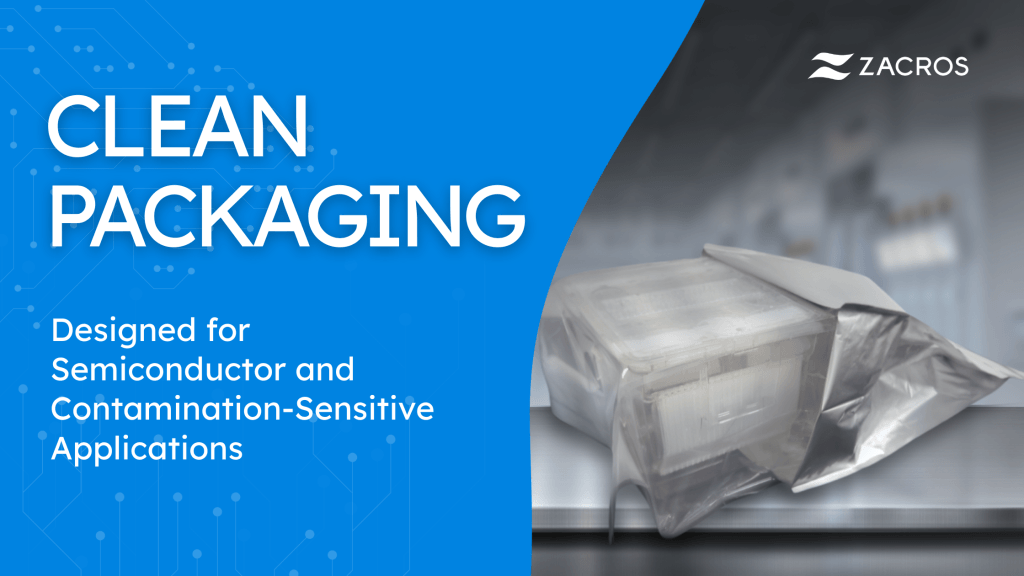
In semiconductor and contamination-sensitive industries, packaging plays a critical role in protecting products not only from the external environment, but also from interactions with the packaging itself. ZACROS’ Clean Pack solutions are designed specifically for this environment.
That foundation dates back to 1914, when ZACROS first began developing film-based products. By the late 1980s, the company had expanded into the information technology sector, supporting Japan’s growing semiconductor industry and wafer manufacturing. Clean Pack is built on decades of advancements in film lamination and material engineering.
Why Clean Packaging Matters in Semiconductor Manufacturing
Semiconductor processes demand extreme precision. Even minor contamination can impact yield, performance, or reliability, as microscopic particles can lead to defects, yield loss, or product failure.
Packaging used in this environment must:
- Minimize impact from the external environment
- Prevent chemical contamination from packaging materials
- Maintain consistent material performance during handling and transport
These same requirements are not limited to semiconductors. Industries such as optics and advanced electronics face similar challenges, where surface defects, particles, or material interactions can directly affect product quality.
The Technology Behind Clean Pack: Advanced Film Lamination
The performance of Clean Pack starts with film design. ZACROS leverages its core lamination technology to control material structure, adhesive selection, and barrier properties.
This level of control is essential for high-purity applications because it enables:
- Reduced generation of extractables or leachables
- Stable performance across production and logistics conditions
- Customization based on application-specific requirements

From Consumer Packaging to High-Purity Applications
ZACROS originally applied lamination technology to flexible packaging, including refill pouches for home & personal care liquid products as well as bulk liquid containers like Cubitainer for food and reagent products.
Over time, this same expertise evolved into more demanding applications such as:
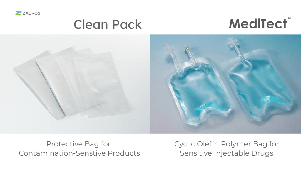
- MediTect (Medical packaging) requiring chemical inertness
- Clean Pack (Semiconductor packaging) requiring clean environments
This evolution reflects a key strength and the ability to apply one core technology, film lamination, across increasingly stringent requirements.
Why Film Technology Matters More Than Ever
As industries continue to advance, tolerances are becoming tighter and materials more sensitive. Packaging is no longer a passive component. It is part of the overall process system.
This shift is driving demand for better control of packaging-material interactions and more consistent packaging quality. ZACROS’ foundation in lamination technology positions Clean Pack to meet these demands because performance is built directly into the film structure.
Conclusion
Clean Pack reflects how ZACROS applies its core film technology to solve high-value, high-risk challenges. In semiconductor manufacturing, where precision is critical, packaging must deliver the same level of control. With decades of experience supporting wafer manufacturing, ZACROS understands the practical requirements of working within semiconductor production environments. Clean Pack was originally designed for wafer carriers such as FOUP, but the technology can be adapted to support a broader range of contamination-sensitive applications. This includes industries such as optics and advanced electronics, where even minimal contamination can impact product performance and quality. Contact us for more information.